行业产品

  • 行业产品

无锡奥本精密工业有限公司


当前位置:无锡奥本精密工业有限公司>>长度类精密计量仪器>>干涉仪>>MicroXAM白光干涉轮廓仪干涉仪

MicroXAM白光干涉轮廓仪干涉仪

返回列表页
参  考  价面议
具体成交价以合同协议为准

产品型号

品       牌

厂商性质其他

所  在  地无锡市

包装印刷网采购部电话:0571-88918531QQ:2568841715

联系方式:查看联系方式

更新时间:2025-03-19 12:11:29浏览次数:32次

联系我时,请告知来自 包装印刷网

产品简介

白光干涉轮廓仪干涉仪产品主要特点:MicroXAM白光干涉轮廓仪干涉仪纳米轮廓仪

详细介绍

白光干涉轮廓仪 干涉仪产品主要特点:

MicroXAM白光干涉轮廓仪干涉仪纳米轮廓仪,微纳米加工测量,苹果(apple)轮廓仪
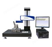


OVERVIEW

The MicroXAM-100 complements our surface profiling portfolio with a research grade, non-contact optical profiler. The MicroXAM-100 is a full-featured white light and

phase-shifting interferometer that brings a powerful set of features and capabilities to the general research community. The system provides precise high-resolution, non-contact 3D profiles on both smooth and rough surfaces. The intuitive user interface allows for a fast learning curve ensuring quick and productive use of the tool in any environment.

The MicroXAM-100 can measure fields of view from 100 X 100 microns to

1.0mm x 1.0mm (dependent on the objective lens used). The MicroXAM-100 optical interferometer quickly and accurately measures the 3D topography of surfaces at the nanometer level with a z-scan range of 250 microns (or up to 10 mm with Z-stitching). Multiple images can be stitched together to produce extended fields of view.


  • PSI (phase) and VSI mode (vertical) with patented noise suppression technology
  • 100 µm closed loop piezo stage and 10mm z-stage for VSI scanning mode
  • Sample stages up to 8" (200mm) with full stage travel
  • X-Y stage options supporting manual, motorized, and programmable 4, 6, and 8" (100, 150, and 200mm)
  • Sequence, Stitching, Thick film thickness, dissimilar materials, and masking measurement modules.
  •  


The MicroXAM-1200 3D non-contact profilometer is a surface characterization solution for a wide range of applications and industries - from R&D departments, universities, and commercial labs to production monitoring and process control in IC manufacturing and data storage. The non-contact profilometer uses white light interferometry to generate high-resolution 3D images that provide the industry’s highest vertical resolution with excellent repeatability and precision, and superior reliability measurements. This surface analysis solution delivers automated data collection, automated analysis and reporting, with 2D or 3D advanced analysis suite to address a variety of application and reporting needs.
 
 
  • PSI (phase) and VSI mode (vertical) with patented noise suppression technology
  • 100 µm closed loop piezo stage and 10mm z-stage for VSI scanning mode
  • Sample stages up to 8" (200mm) with full stage travel
  • X-Y stage options supporting manual, motorized, and programmable 4, 6, and 8" (100, 150, and 200mm)
  • Sequence, Stitching, Thick film thickness, dissimilar materials, and masking measurement modules.
 

MicroXAM白光干涉轮廓仪干涉仪

The precision engineered hardware along with powerful yet simple to use MapVUE® AE analysis software package offers the user a number of parameter calculations, filtering options, imaging analysis and automated report generation to meet the most stringent R&D and production environment needs. MapVUE AE’s user interface offers simple recipe development, automated sequencing, and with a range of analysis tools. The flexibility of the instrument is further demonstrated with its mix of objectives and sample stages available to meet the need of each application with customization.

 
APPLICATIONS
 
Medical Devices

MicroXAM白光干涉轮廓仪干涉仪

Surface texture, defect inspection, wear volume measurement and film thickness measurement of medical implants such as heart-valves, artificial joints, dental implants and stents.

 
Precision Machining
Wear on cylindrical surface, grain structure analysis, surface roughness characterization and form measurement
 
Data Storage
 
LED
Sapphire substrate roughness, waviness and edge roll-off; patterned sapphire bump height and width; defect characterization, and step height for photo resist and metallization
 
Semiconductors and Electronics
Wafer inspection including height of through silicon via and bond pads, height of deposition and etch steps film thickness, critical dimension measurement
Optics
Surface pattern and feature dimensions of holographic elements, micro-lens arrays, gem surface facet surface analysis and critical dimensioning, fiber optics connector end-face, etch performance and mask quality.
 

MEMS

MicroXAM白光干涉轮廓仪干涉仪


Shape, surface detail and defect features of MEMS sensors, actuators, deformable optics and pumps. Non contact process allows in situ measurement of activated structures.
MicroXAM白光干涉轮廓仪干涉仪

 MicroXAM白光干涉轮廓仪干涉仪


感兴趣的产品PRODUCTS YOU ARE INTERESTED IN

包装印刷网 设计制作,未经允许翻录必究 .      Copyright(C) 2021 https://www.ppzhan.com,All rights reserved.

以上信息由企业自行提供,信息内容的真实性、准确性和合法性由相关企业负责,包装印刷网对此不承担任何保证责任。 温馨提示:为规避购买风险,建议您在购买产品前务必确认供应商资质及产品质量。

会员登录

×

请输入账号

请输入密码

=

请输验证码

收藏该商铺

登录 后再收藏

提示

您的留言已提交成功!我们将在第一时间回复您~